The article discusses various microcircuits of the output stages of the vertical scan. Many microcircuits have already been discontinued, but are still available in the Dalincom online store and other radio stores.
1. Microcircuits from SANYO
1.1. LA7837, LA7838
Microcircuits LA7837, LA7838 can be used as output stages of vertical scanning in TVs and monitors. LA7837 is intended for portable TVs and TVs of the middle class, with a maximum current of the frame coils of the deflection system of kinescopes of no more than 1.8 A. For TVs with 33 ... 37 "kinescope diagonals, the LA7838 is intended with a maximum deflection current of 2.5 A. The microcircuits are produced in the SIP13H case ... The pinout of the microcircuit is shown in Fig. 1. The microcircuits include an input trigger, a sawtooth driver, a size switching circuit, an output amplifier, a booster circuit for generating a flyback pulse, and a thermal protection circuit. The block diagram of the microcircuits is shown in Fig. 2.

The frame sync signal is fed to the trigger input of the microcircuit (pin 2). At the output of the trigger, pulses are formed, the frequency of which corresponds to the vertical scan frequency. An external circuit connected to the pin. 3, determines the initial moment of the formation of the sawtooth signal. The sawtooth signal is formed using an external capacitor connected to the pin. 6. The change in the amplitude of the signal of the vertical saw is made using a size switching circuit based on an external identification signal with a frequency of 50/60 Hz and using a feedback signal coming to the pin. 4. The feedback signal, proportional to the amplitude of the output signal, is removed from the external current-limiting resistor connected in series with the frame coils of the OS. The generated frame saw signal is fed to the frame scan signal amplifier, while the gain and linearity of the stage depend on the feedback signal supplied to the pin. 7.

The output stage of the microcircuit generates directly the deflection current (pin 12). To power it, a voltage boost circuit with an external capacitor and a diode is used. During the forward run, the output stage is powered through an external diode with the voltage supplied to the pin. 8. During the reverse stroke, the voltage stored on the external boost capacitor is added to the supply voltage using the reverse pulse shaping circuit. As a result, approximately twice the voltage is applied to the output stage of the microcircuit. In this case, a reverse pulse is formed at the output of the cascade, which exceeds the supply voltage of the microcircuit in amplitude. To block the output stage, a pin is used. 10. Characteristics of microcircuits are given in table. 1.
1.2. LA7845

The LA7845 microcircuit is used as a vertical scan output stage in TVs and monitors with 33 ... 37 ”CRT diagonals and a maximum deflection current of 2.2 A. The microcircuit is produced in a SIP7H package. The pinout of the microcircuit is shown in Fig. 3. The microcircuit includes an output amplifier, a voltage boost circuit for generating a reverse pulse and a thermal protection circuit. The block diagram of the microcircuit is shown in Fig. 4.

The frame saw signal is fed to the frame scan signal amplifier (pin 5). The same pin receives a feedback signal that determines the gain and linearity of the stage. A reference voltage is supplied to the other input of the amplifier (pin 4). At the output of the amplifier (pin 2), a deflection current is formed. A boost circuit with an external capacitor and a diode is used to power the output stage of the amplifier during the flyback. The characteristics of the microcircuit are given in table. 2.
1.3. LA7875N, LA7876N

Microcircuits LA7875N, LA7876N are intended for use in TVs and monitors with high resolution. The microcircuit is produced in SIP10H-D and SIP10H cases, respectively. The pinout of the microcircuits is shown in Fig. 5 and 6. The microcircuits include an output amplifier, two voltage boost circuits and a thermal protection circuit. The maximum output current of the LA7875N microcircuit is 2.2 A, and the LA7876N - 3 A. The block diagram of the microcircuits is shown in Fig. 7.

To reduce the vertical retrace time required to increase the resolution, the microcircuit uses two voltage boost circuits. This makes it possible to increase the supply voltage of the output stage during the reverse stroke by three times, which accordingly leads to an increase in the amplitude of the output pulse of the reverse stroke.

The frame saw signal is fed to the inverting input of the vertical scan signal amplifier (pin 6). A feedback signal is sent to the same pin. A reference voltage is supplied to the direct input of the amplifier (pin 5). To power the output stage of the amplifier during the reverse stroke, two voltage boost circuits are used, which increase the supply voltage of the output stage three times. The characteristics of the microcircuits are given in table. 3.
1.4. STK792-210

The STK792-210 microcircuit is intended for use as a vertical output stage in high-resolution TVs and monitors. The microcircuit is produced in the SIP14C3 package. The pinout of the microcircuit is shown in Fig. 8. The microcircuit includes an output amplifier, a voltage boost circuit for generating a reverse pulse, a built-in voltage boost circuit diode and a vertical alignment circuit. The block diagram of the microcircuit is shown in Fig. nine.

The signal of the vertical saw through an external amplifier goes to the amplifier of the vertical scan signal (pin 12). At the input of an external amplifier, this signal is added to the feedback signal, which determines the gain of the entire vertical scan channel and its linearity. The other input of the external amplifier is supplied with a reference voltage and a local feedback signal. The deflection current is formed at the output of the amplifier (pin 4). To power the output stage of the amplifier during the reverse stroke, a voltage boost circuit with a built-in diode and an external capacitor is used (pin 6 and 7). The built-in vertical alignment scheme is used to adjust the alignment. Alignment is carried out by changing the potential of a constant level on the pin. 2. The characteristics of the microcircuit are given in table. 4.
1.5. STK79315A
The STK79315A microcircuit is designed for use in monitors with high resolution as a vertical output stage. The microcircuit is produced in a SIP18 package. The pinout of the microcircuit is shown in Fig. 10. The microcircuit includes a frame frequency generator, a sawtooth signal shaper, an output amplifier, a voltage boost circuit for generating a reverse pulse, a built-in voltage boost circuit diode and a vertical alignment circuit. The block diagram of the microcircuit is shown in Fig. eleven.

The TTL level signal is fed to the synchronization input of the frame rate generator (pin 18). The external circuit of the generator is connected to the pin. 16. The output signal of the generator goes to the sawtooth signal shaping circuit. The external capacitor of the driver is connected to the pin. 11. The feedback circuit of the driver, which determines the linearity of the output signal, is connected to the pin. 14. The amplitude of the saw signal is determined by the potential at the pin. 12. From the output of the shaper, the frame saw signal is fed to the frame scan signal amplifier. A feedback signal is sent to the other input of the amplifier from external circuits, which determines the gain of the stage and its linearity. After amplification, the vertical ramp signal is fed to the output stage. At the output of the output stage (pin 3), a deflection current is generated. To power the output stage during the reverse run, a voltage boost circuit with a built-in diode and an external capacitor is used (pin 5 and 6). The voltage boost circuit is controlled by output pulses through the pin. 4 microcircuits. The built-in vertical alignment scheme is used to adjust the alignment. Alignment is carried out by changing the potential of a constant level at pin 2. The characteristics of the microcircuit are given in table. five.
2. Microcircuits from SGS THOMSON
2.1. TDA1771
.png)
The TDA1771 microcircuit is used in TVs and monitors as a vertical output stage. The microcircuit is produced in a SIP10 package. The pinout of the microcircuit is shown in Fig. 12. The microcircuit includes a sawtooth signal shaper, an output amplifier, a voltage boost circuit for generating a reverse pulse and a thermal protection circuit. The block diagram of the microcircuit is shown in Fig. 13.
.png)
The frame sync signal of negative polarity is fed to the frame saw driver (pin 3). To pin. 6, the capacitor of the driver is connected, and the amplitude of the signal at the output of the driver is adjusted using a circuit connected to the pin. 4. Formed sawtooth signal through the buffer stage and pin. 7 and 8 is fed to the vertical signal amplifier. The same input of the amplifier receives a feedback signal that determines the gain and linearity of the output stage. The other input of the amplifier (direct) is supplied with a reference voltage from an internal voltage regulator. At the output of the amplifier (pin 1), a deflection current is formed. A boost circuit with an external capacitor and a diode is used to power the output stage of the amplifier during the flyback. The characteristics of the microcircuit are given in table. 6.
2.2. TDA8174, TDA8174W
.png)
Microcircuits TDA8174, TDA8174W, TDA8174A are used as the frame output stage in TVs and monitors. The microcircuits are available in MULTIWATT11 and CLIPWATT11 packages, respectively. The pinout of the microcircuits is shown in Fig. 14 and 15. The microcircuits include a sawtooth signal driver, an output amplifier, a booster circuit for generating a reverse pulse, and a thermal protection circuit. The block diagram of the microcircuit is shown in Fig. sixteen.
.png)
The frame sync signal of negative polarity is fed to the frame saw driver (pin 3). To pin. 7, the capacitor of the driver is connected, and the amplitude of the signal at the output of the driver is adjusted using a circuit connected to the pin. 4. Formed sawtooth signal through the buffer stage and pin. 8 and 9 is fed to the frame scan signal amplifier. The same pin receives a feedback signal that determines the gain and linearity of the output stage. The other input of the amplifier (direct) is supplied with a reference voltage from an internal voltage regulator. At the output of the amplifier (pin 1), a deflection current is formed. A boost circuit with an external capacitor and a diode is used to power the output stage of the amplifier during the flyback. The characteristics of the microcircuit are given in table. 7.
2.3. Functional features of SGS THOMSON microcircuits
.png)
As a sawtooth signal shaper in SGS THOMSON microcircuits, a shaper is used, the diagram of which is shown in Fig. 17. The sawtooth signal is obtained by charging the external capacitor C with a constant current from the internal current source Iх. The sawtooth signal formed on the capacitor is fed through the buffer stage to the input of the frame scan signal amplifier of the microcircuit. The buffer stage has a low output impedance. During the charging of the capacitor, the voltage at the output of the buffer stage rises until the key T1 closes, controlled by frame sync pulses. After the key is closed, the capacitor is quickly discharged. When the voltage level Umin at the output of the buffer stage is reached, the switch opens and the charging process is repeated. The signal amplitude is adjusted by changing the value of the capacitor charging current.
.png)
The powerful output stage of the microcircuit is designed to generate a deflection current in personnel coils with values \u200b\u200bfrom 1 to 3 A and a reverse voltage up to 60 V. A typical circuit of the output stage is shown in Fig. 18. The output stage works as follows. During the first part of the sweep period, the power transistor Q2 is on and current flows through it from the power source to the frame coils of the OS. In the second half of the sweep period, the energy accumulated in the personnel coils forms a reverse current flowing from the personnel coils through the open transistor Q8. To maintain a high level of the flyback pulse at the amplifier output, Q8 is blocked by Q7 during the flyback time.
.png)
To shorten the flyback time, the voltage on the frame coils during the beam return time should be greater than the voltage during the sweep. The increase in the supply voltage of the output stage during the return stroke is carried out using the return driver.
.png)
A typical circuit of the return driver is shown in Fig. 18. The shape of the current through the frame coils and the voltage across them during the frame scan are shown in Fig. 19. During the sweep period (see Fig. 19, t6 - t7), the transistors Q3, Q4 and Q5 of the driver are closed, and the transistor Q6 is in saturation (Fig. 20). In this case, the current flows from the power supply through DB, CB and Q6 to case, charging the capacitor CB to the value UCB \u003d US - UDB - UQ6 (us). At the end of this period, the current reaches its peak value, after which it changes sign and then flows from the frame coils to the output stage. At the same time, the voltage across the UA frame coils reaches its minimum value.
.png)
At the beginning of the formation of the reverse stroke (see Fig. 19 t0 - t1), the output stage transistor Q8, which was previously in saturation, turns off and the current generated by the energy accumulated in the personnel coils flows through the damping circuit and elements D1, CB and Q6 ... The paths of current flow are explained in Fig. 21. When the voltage at point A exceeds the value US (see Figure 19, t1 - t2), transistor Q3 turns on and transistors Q4 and Q5 saturate. As a result, Q6 turns off. During this period, the voltage at point D reaches the value UD \u003d US - UQ4 (us). Thus, the voltage at point B (the supply voltage of the output stage) becomes:
.png)
UB \u003d UCB + UD or
UB \u003d UCB + US - UQ4 (us).
.png)
After reaching the voltage UD \u003d US - UQ4 (us) at point D, the transistor Q4 closes and at time t2 - t3 energy is returned due to the current flow from the personnel coils through D1, CB and D2 to the power source (see Fig. 22) ... The flowing current charges the capacitor CB. At time t3-t4, the current flowing through the personnel coils drops to zero, while the diode D1 closes. After the transition of the transistor of the output stage Q2, according to the signal from the buffer stage, transistors Q3 and Q4 open to saturation (time t4 - t5). As a result, current from the power supply begins to flow through the frame coils through Q4, CB and Q2. The supply voltage at the Q2 collector is UB \u003d UCB + US - UQ4 (us), i.e. almost double the value of the power supply. The flow of current is illustrated in Fig. 23.
.png)
This process continues until the signal from the buffer stage turns off the transistor Q2 of the output stage. When the voltage at point A reaches the value of the supply voltage US (see fig. 19, t5 - t6), the flyback generator is blocked. In this case, the transistor Q3 turns off and turns off the transistor Q4, which makes the connection between point D and C (US). Therefore, UB is reduced to the value UB \u003d US - UDB.
3. Microcircuits from PHILIPS
3.1. TDA8354Q
The TDA8354Q microcircuit is a vertical output stage circuit for use in televisions with deflecting systems 90 and 110 °. The bridge output stage of the microcircuit allows you to process input signal frequencies from 25 to 200 Hz, as well as use deflection coils for CRTs with an aspect ratio of 4: 3 and 16: 9. The microcircuit is available in DIL13 and SIL13 packages. The pinout of the microcircuit is shown in Fig. 24. The block diagram is shown in fig. 25. The microcircuit uses a combined Bipolar, CMOS and DMOS technology.

The standard output stages require the frame deflection coils to be connected via an expensive electrolytic capacitor with a capacity of about 2200 μF, which prevents DC from flowing through the frame coils. However, apart from the higher cost, the coupling capacitor results in image bouncing when switching channels. The TDA8354Q's output stage bridge circuit allows vertical deflection coils to be connected directly to the amplifier outputs without a coupling capacitor, thereby eliminating the aforementioned bouncing and making it easier to stabilize the vertical image position by controlling a small DC current.

The frame deflection coils are connected to the antiphase outputs of the output stage (pin 9 and 5) in series with the measuring resistor RM. The voltage across this resistor is proportional to the current flowing. Negative feedback is used to stabilize the amplitude of the output current (Fig. 25). The feedback voltage is removed from the RM resistor and through the RCON resistor connected in series to the input of the voltage / current converter. The output signal of the converter goes to the input of the output amplifier A of the bridge circuit. The values \u200b\u200bof the RM and RCON resistors determine the gain of the microcircuit's output stage. By changing the values \u200b\u200bof these resistors, you can set the value of the output current from 0.5 to 3.2 A.
An additional power supply UFLB is used to power the microcircuit during the reverse run (pin 7). The additional voltage is connected during the return stroke by an internal switch. The absence of a blocking capacitor allows this voltage to be directly applied to the personnel coils.
The reverse switch is turned off when the output current reaches the set value. The output current is then formed by stage A. The output voltage is reduced to the level of the main supply voltage.
The microcircuit protection circuit is used to generate a protection signal in the event of a frame scan malfunction to prevent burn-through of the kinescope phosphor. The protection circuit also generates a blanking signal (pin 1) during the reverse stroke, which can be used together with the SC (sandcastle) signal to synchronize the video processor. The protection circuit forms an active high level on the pin. 1 during the reverse stroke, as well as in the following cases:
• open circuit of personnel deflecting coils (idle);
• the feedback loop is open;
• absence of a sweep signal;
• activation of thermal protection (T \u003d 170 ° C);
• pin closure. 5 or 9 per power supply bus;
• pin closure. 5 or 9 for a common conductor;
• closure of input pins. 11 or 12 per power supply bus;
• closure of input pins. 11 or 12 for a common conductor;
• short circuit in deflecting coils.

In the absence of a sweep signal or a short circuit in the frame coils, the protection signal is generated with a delay of about 120 ms. This is necessary when operating with signals with a minimum frequency of 25 Hz to correctly detect and hold the retrace signal.
In parallel with the deflection coils, a damping resistor RP is included to limit the oscillatory process in the personnel coils. The current flowing through this resistor in sweep and flyback mode has a different value. In this case, the current flowing through the measuring resistor RM consists of the current flowing through the resistor RP and the current flowing through the frame coils. This leads to a decrease in the current flowing through them at the beginning of the sweep process. To compensate for the change in current flowing through the measuring resistor over time, caused by the current through the damping resistor, an external compensating resistor Rcomp is used, connected to the output of the compensation circuit (pin 13) and the output of amplifier A (pin 9).

The input amplifier of the TDA8354Q microcircuit is designed to work with synchroprocessors that form a differential sawtooth signal of a vertical scan, with a reference level of constant voltage. The signal from the amplifier output goes to one of the inputs of the voltage / current converter (Fig. 26). A feedback signal comes to the same input of the converter, which is removed through the RCON resistor (pin. 3). The voltage taken from the measuring resistor RM is applied to the other output of the converter through the RS resistor. The output of the converter is proportional to the voltage applied to the inputs of the converter. Thus, with a closed feedback loop, the device tends to equalize the potential at the pin. 2 microcircuits in relation to the potential on the pin. 3.

The output stage of the microcircuit consists of two identical amplifiers connected in a bridge circuit (Fig. 27). The frame deflection coils and the measuring resistor are connected to the outputs of the amplifiers (pin 9 and 5). In the first part of the vertical sweep period, the sawtooth current flows through transistor Q2, diode D3, personnel coils, measuring resistor RM, and transistor Q5. In this case, power is supplied through the pin. 10 microcircuits. The current flowing through the frame coils, which is maximum at the beginning of the period, will decrease linearly as the beam approaches the middle of the screen. In the second part of the sweep period, the current flows through transistor Q4, measuring resistor RM, frame coils and transistor Q3. Power in this case is carried out from the same source, but through the pin. 4. In this case, the current flowing through the frame coils changes direction and increases linearly towards the end of the sweep period. The operation of the output stage during the sweep period is explained in Fig. 28.

During the reverse stroke, the current flowing through the frame coils should change from a minimum to a maximum value in a short time... Power during the return stroke is carried out from the pin. 7 through the reverse switch - transistor Q1. To decouple the two power supplies, diodes D2 and D3 are additionally included in the output stages of the microcircuit.
The formation of the reverse current is carried out in two stages. At the first stage (1), the current, due to the energy accumulated in the personnel coils, flows from the power source (pin 4) through the Q4 transistor, the measuring resistor RM, the personnel coils, the diode D1 and the capacitor of the reverse power circuit (see Fig. 27 ). In this case, the capacitor is charged with voltage on the pin. 9. The maximum voltage on the pin. 9 will be 2 V greater than the supply voltage of the flyback source. The operation of the output stage during the reverse sweep is illustrated in Fig. 29.
The second stage of formation of the reverse stroke begins from the moment when the current flowing through the frame coils passes through the zero level. The current through the personnel coils then flows from the reverse source (pin 7), transistor Q1, diode D2, personnel coils, measuring resistor RM, transistor Q5. Due to the voltage drop across the transistor Q1 and diode D2, the voltage across the pin. 9 will be 2 ... 8 V less than the power supply voltage. The current through the frame coils increases to a value corresponding to the input signal level. Then Q1 turns off and a new sweep begins.
3.2 TDA8356
The TDA8356 vertical output stage microcircuit is designed for use in televisions with deflecting systems of 90 and 110 degrees. The bridge output stage of the microcircuit allows the use of sweep signals with frequencies from 50 to 120 Hz. The microcircuit is manufactured in a SIL9P package. The pinout of the microcircuit is shown in Fig. 30. The block diagram of the microcircuit is shown in fig. 31.

The input stage of the microcircuit is designed to work with synchroprocessors that form a differential sawtooth signal of a vertical scan, which is fed to the pin. 1 and 2. In this case, the reference level of the constant voltage is formed by the reference voltage source of the microcircuit. An external RCON resistor connected between the two differential inputs determines the current through the vertical deflection coils. The dependence of the output current on the input current is defined as:
IinґRCON \u003d IoutRM, where Iout is the current through the frame deflection coils.

The maximum peak-to-peak amplitude of the input voltage is 1.8V (1.5V typical). The output bridge circuit allows you to connect the frame deflection coils directly to the outputs of the amplification stages (pins 7 and 4). To control the current flowing through the frame coils, a resistor RM is connected in series with them. The voltage generated across this resistor through the pin. 9 of the microcircuit is fed to a feedback signal amplifier, which limits the value of the output current. By changing the RM value, the maximum output current can be set from 0.5 to 2 A.
To power the output stage during the reverse run, a separate source with increased voltage is used (pin 6). The absence of a blocking capacitor in the output circuits makes it possible to use this voltage more efficiently, since all this voltage will be directly applied to the frame deflection coils during the reverse stroke.

The microcircuit has a number of protective functions. To provide safe work the output stage is:
Thermal protection;
Short circuit protection between the pin. 4 and 7;
Protection against short circuit of power supplies.
To quench the kinescope, the built-in quenching circuit generates a signal in the following cases:
During the reverse motion of the vertical scan;
With a short circuit between the pin. 4 and 7 or power supplies per case;
With an open feedback loop;
When the thermal protection is activated.
The main parameters of the microcircuit are given in table. eight.
3.3 TDA8357
The TDA8357 microcircuit is intended for use in televisions with deflecting systems of 90 and 110 degrees. The bridge output stage of the microcircuit allows the use of a microcircuit with signal frequencies from 25 to 200 Hz, as well as the use of deflection coils for picture tubes with an aspect ratio of 4: 3 and 16: 9. The microcircuit is produced in the DBS9 package. The pinout of the microcircuit is shown in Fig. 32, and its structural diagram is shown in Fig. 33. The microcircuit uses a combined Bipolar, CMOS and DMOS technology.

The input stage of the microcircuit is designed to work with synchroprocessors that generate a differential sawtooth signal of a vertical scan with a reference level of constant voltage. In this case, the dependence of the output current on the input current is defined as:
2ґIinRin \u003d IoutґRM, where Iout is the current through the frame deflection coils.
The maximum peak-to-peak amplitude of the input voltage is 1.6 V.
The frame deflection coils, connected in series with the measuring resistor RM, are connected to the antiphase outputs of the output stage (pin 7 and 4). Negative feedback is used to stabilize the amplitude of the output current. The feedback voltage is removed from the resistor RM and, through the resistor RS, is fed to the input of the voltage / current converter, the output signal of which is fed to the input of the output amplifier of the bridge circuit. The values \u200b\u200bof the resistors RM and RS determine the gain of the output stage of the microcircuit. By changing the values \u200b\u200bof these resistors, you can set the value of the output current from 0.5 to 2 A.

In parallel with the deflection coils, a damping resistor RP is included, which limits the oscillatory process in the personnel coils. The currents flowing through this resistor during forward and reverse travel have different meanings. The current flowing through the measuring resistor RM consists of the current flowing through the resistor RP and the current flowing through the frame coils. An external compensating resistor Rcomp is used to compensate for the change in current through the measuring resistor caused by different currents through the damping resistor at the beginning and end of the sweep. An external compensating resistor is connected between the pin. 7 and 1. In this case, the source of the compensation current is a constant reference voltage at the pin. 1. To prevent the influence of the output voltage on the input circuit, a diode is connected in series with the resistor.
An additional VFB power supply (pin 6) is used to power the microcircuit during the reverse run. The connection of this voltage during the return stroke is carried out by an internal switch. The absence of a decoupling capacitor allows this voltage to be directly applied to the personnel coils. The reverse switch closes when the output current reaches the set value.
The microcircuit protection circuit is used to block the output stage of the microcircuit in conditions of thermal protection actuation and overload of the output stage. The microcircuit protection circuit generates a blanking signal (pin 8), which can be used together with the SC (sandcastle) signal to synchronize the video processor. Active high level on pin. 8 is formed during the reverse stroke, if the feedback circuit is open and when thermal protection is activated (T \u003d 170 ° C).
The main parameters of the microcircuit are given in table. nine.
3.4 TDA8358
The TDA8358 microcircuit is intended for use in televisions with deflecting systems of 90 and 110 degrees as a vertical output stage and an amplifier for geometric distortion correction signals. The bridge output stage of the microcircuit allows the use of a microcircuit with signal frequencies from 25 to 200 Hz, as well as the use of deflection coils for picture tubes with an aspect ratio of 4: 3 and 16: 9. The microcircuit is produced in the DBS13 package. The pinout of the microcircuit is shown in Fig. 34, and its structural diagram is shown in Fig. 35. The microcircuit is manufactured using the combined technology of Bipolar, CMOS and DMOS.

The microcircuit contains a sweep unit similar to the TDA8357J. The difference lies in the presence of a compensation circuit that forms the voltage for the compensation resistor Rcomp. In addition, the microcircuit includes an amplifier for correcting geometric distortions. The correction signal amplifier is designed to amplify the correction current and directly control the diode modulator of the line scan output stage circuit. The amplifier must have negative feedback for proper operation. The feedback circuit is connected between the output and input terminals of the amplifier. The maximum output voltage of the amplifier should not exceed 68 V, and the maximum output current should not exceed 750 mA.
The main parameters of the microcircuit are given in table. ten.
4.Circuits from TOSHIBA4.1 TA8403K, TA8427K

Microcircuits TA8403K and TA8427K are used as a vertical output stage in TVs with a maximum deflection current in the frame coils of picture tubes of no more than 1.8 and 2.2 A (for TA8427K). The microcircuits are produced in the HSIP7 package. The pinout of the microcircuits is shown in Fig. 36. Microcircuits include a preliminary and output amplifiers and a voltage boost circuit for forming reverse pulses. The block diagram of the microcircuits is shown in Fig. 37.

The vertical scan signal is fed to the input of the pre-amplifier (pin 4) and, after amplification, is fed to the output stage, where the deflection current is formed (pin 2). A voltage boost circuit with an external capacitor and a diode is used to power the output stage. During the forward run, the output stage is powered through an external diode with the voltage supplied to the pin. 6 microcircuits. During the reverse stroke, the voltage accumulated on the external boost capacitor is added to the supply voltage using the reverse pulse shaping circuit. This voltage is applied to the pin. 3 microcircuits. In this case, reverse pulses are formed at the output of the cascade, which exceed the supply voltage of the microcircuit in amplitude. The main characteristics of microcircuits are given in table. 11 (values \u200b\u200bfor the TA8427K microcircuit are shown in brackets).
4.2 TA8432K
The TA8432K microcircuit is a vertical output stage with the formation of a frame saw signal. The microcircuit is produced in the HSIP12 package and is used in TVs with a maximum deflection current in the frame coils of picture tubes of not more than 2.2 A. The arrangement of the microcircuit terminals is shown in Fig. 38. The microcircuit includes: an input trigger, a sawtooth signal shaper, an output amplifier and a reverse pulse shaping circuit.

The block diagram of the microcircuit is shown in Fig. 39.

The frame sync pulses are fed to the trigger input (pin 2), the output of which is connected to the sawtooth signal shaper. The formation of the sawtooth signal is carried out using an external capacitor connected to the pin. 5. Changing the amplitude of the frame saw signal is made using a circuit connected to the pin. 3 microcircuits. The generated signal of the personnel saw goes to the pre-amplifier, while the gain and linearity of the stage depend on the feedback signal coming to the pin. 6 microcircuits. The output stage generates directly the deflection current (pin 11). To power the output stage, a voltage boost circuit with an external capacitor and a diode is used. During the forward run, the output stage is powered through an external diode with the voltage supplied to the pin. 7 microcircuits. During the reverse stroke, the voltage accumulated on the external boost capacitor is added to the supply voltage using the reverse pulse shaping circuit. As a result, approximately twice the voltage is applied to the output stage of the microcircuit. In this case, reverse pulses are formed at the output of the cascade, which exceed the supply voltage of the microcircuit in amplitude. The main characteristics of the microcircuit are given in table. 12.
4.3 TA8445K

The TA8445K microcircuit is similar to the TA8432K microcircuit in terms of its characteristics and scope. A distinctive feature is that a 50/60 Hz switching unit is additionally introduced into this microcircuit. The switching signal is fed to the pin. 4 microcircuits. The block diagram of the microcircuit is shown in Fig. 40.
They are a thing of the past, and now, in order to assemble any simple amplifier, you no longer have to suffer with calculations and rivet a large printed circuit board.
Nowadays, almost all cheap amplifying equipment is made on microcircuits. The most widely used TDA chips for amplifying the audio signal. They are currently used in car radios, active subwoofers, home speakers, and many other audio amplifiers, and look something like this:


Pros of TDA chips
- In order to assemble an amplifier on them, it is enough to supply power, connect speakers and several radio elements.
- The dimensions of these microcircuits are very small, but you will have to put them on the radiator, otherwise they will get very hot.
- They are sold at any radio store. On Ali, something is expensive if you take it at retail.
- They have built various protections and other options, such as mute, etc. But according to my observations, the protections do not work very well, therefore microcircuits often die either from overheating, or from. So it is advisable not to close the microcircuit terminals with each other and not to overheat the microcircuit, squeezing all the juices out of it.
- Price. I would not say that they are very expensive. They have no equal in terms of price and functions.
Single-channel amplifier on TDA7396
Let's build a simple one-channel amplifier based on the TDA7396 chip. At the time of this writing, I took it at a price of 240 rubles. The datasheet on the microcircuit said that this microcircuit can deliver up to 45 watts into a 2 Ohm load. That is, if you measure the resistance of the speaker coil and it will be about 2 ohms, then on the speaker it is quite possible to get a peak power of 45 watts.This power is quite enough to arrange a disco in a room not only for yourself, but also for neighbors and at the same time get a mediocre sound, which, of course, cannot be compared with hi-fi amplifiers.
Here is the pinout of the microcircuit:

We will assemble our amplifier according to the typical scheme, which was attached in the datasheet itself:

We serve + Vs on leg 8, and do not serve anything on leg 4. Therefore, the diagram will look like this:

Vs is the supply voltage. It can be between 8 and 18 volts. “IN +” and “IN-” - we send a weak sound signal here. We hook the speaker to the 5th and 7th legs. We put the sixth leg on the minus.
Here is my surface mount assembly

I did not use capacitors at the power input 100nF and 1000uF, since I have a pure voltage from the power supply.
I rocked the speaker with the following parameters:

As you can see, the resistance of the coil is 4 Ohms. The frequency band indicates that it is a subwoofer type.
And this is how my sub looks like in a self-made case:

I tried to shoot a video, but the sound on the video is very poor. But all the same, I can say that from the phone at medium power it was already hammering so that the ears were wrapped up, although the consumption of the entire circuit in working form was only about 10 watts (multiply 14.3 by 0.73). In this example, I took the voltage as in a car, that is, 14.4 Volts, which is well within our operating range from 8 to 18 Volts.

If you do not have a powerful power source, then you can assemble it according to this scheme.
Do not dwell on this particular microcircuit. There are many types of these TDA microcircuits, as I said. Some of them amplify the stereo signal and can output sound to 4 speakers at once, as is done in car radios. So do not be too lazy to rummage on the Internet and find a suitable TDD. After completing the assembly, let the neighbors check out your amplifier by unscrewing the volume knob for the whole balalaika and leaning the powerful speaker against the wall).
But in the article I assembled an amplifier on a TDA2030A microcircuit

It turned out very well, since the TDA2030A has better characteristics than the TDA7396
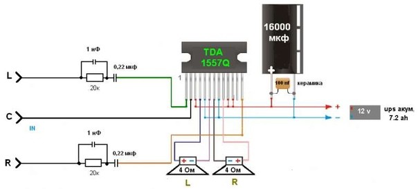
I will also attach, for a change, another diagram from a subscriber whose amplifier on the TDA 1557Q has been working properly for more than 10 years in a row:
Amplifiers on Aliexpress
On Ali, I also found whale kits on TDA. For example, this stereo amplifier is 15 watts per channel for $ 1. This power is quite enough to hang out with your favorite tracks in the room.

You can buy.
And here it is ready right away

Anyway, there are a lot of these amplifier modules on Aliexpress. Click on this link and choose any amplifier you like.
3.2 TDA8356
The TDA8356 vertical output stage microcircuit is designed for use in televisions with deflecting systems of 90 and 110 degrees. The bridge output stage of the microcircuit allows the use of sweep signals with frequencies from 50 to 120 Hz. The microcircuit is manufactured in a SIL9P package. The pinout of the microcircuit is shown in Fig. 30. The block diagram of the microcircuit is shown in fig. 31.
The input stage of the microcircuit is designed to work with synchroprocessors that form a differential sawtooth signal of a vertical scan, which is fed to the pin. 1 and 2. In this case, the reference level of the constant voltage is formed by the reference voltage source of the microcircuit. An external RCON resistor connected between the two differential inputs determines the current through the vertical deflection coils. The dependence of the output current on the input current is defined as:
IinґRCON \u003d IoutRM, where Iout is the current through the frame deflection coils.
The maximum peak-to-peak amplitude of the input voltage is 1.8V (1.5V typical). The output bridge circuit allows you to connect the frame deflection coils directly to the outputs of the amplification stages (pins 7 and 4). To control the current flowing through the frame coils, a resistor RM is connected in series with them. The voltage generated across this resistor through the pin. 9 of the microcircuit is fed to a feedback signal amplifier, which limits the value of the output current. By changing the RM value, the maximum output current can be set from 0.5 to 2 A.
To power the output stage during the reverse run, a separate source with increased voltage is used (pin 6). The absence of a blocking capacitor in the output circuits makes it possible to use this voltage more efficiently, since all this voltage will be directly applied to the frame deflection coils during the reverse stroke.
The microcircuit has a number of protective functions. To ensure safe operation of the output stage, these are:
• thermal protection;
• protection against short circuit between pin. 4 and 7;
• protection against short circuit of power supplies.
To quench the kinescope, the built-in quenching circuit generates a signal in the following cases:
• during the reverse course of the vertical scan;
• with a short circuit between the pin. 4 and 7 or power supplies per case;
• with an open feedback circuit;
• when the thermal protection is activated.
The main parameters of the microcircuit are given in table. eight.
3.3 TDA8357J
The TDA8357J microcircuit is intended for use in televisions with deflecting systems of 90 and 110 degrees. The bridge output stage of the microcircuit allows the use of a microcircuit with signal frequencies from 25 to 200 Hz, as well as the use of deflection coils for picture tubes with an aspect ratio of 4: 3 and 16: 9. The microcircuit is produced in the DBS9 package. The pinout of the microcircuit is shown in Fig. 32, and its structural diagram is shown in Fig. 33. The microcircuit uses a combined technology Bipolar, CMOS and DMOS.
The input stage of the microcircuit is designed to work with synchroprocessors that generate a differential sawtooth signal of a vertical scan with a reference level of constant voltage. In this case, the dependence of the output current on the input current is defined as:
2ґIinRin \u003d IoutґRM, where Iout is the current through the frame deflection coils.
The maximum peak-to-peak amplitude of the input voltage is 1.6 V.
The frame deflection coils, connected in series with the measuring resistor RM, are connected to the antiphase outputs of the output stage (pin 7 and 4). Negative feedback is used to stabilize the amplitude of the output current. The feedback voltage is removed from the resistor RM and, through the resistor RS, is fed to the input of the voltage / current converter, the output signal of which is fed to the input of the output amplifier of the bridge circuit. The values \u200b\u200bof the resistors RM and RS determine the gain of the output stage of the microcircuit. By changing the values \u200b\u200bof these resistors, you can set the value of the output current from 0.5 to 2 A.
In parallel with the deflection coils, a damping resistor RP is included, which limits the oscillatory process in the personnel coils. The currents flowing through this resistor during forward and reverse travel have different meanings. The current flowing through the measuring resistor RM consists of the current flowing through the resistor RP and the current flowing through the frame coils. An external compensating resistor Rcomp is used to compensate for the change in current through the measuring resistor caused by different currents through the damping resistor at the beginning and end of the sweep. An external compensating resistor is connected between the pin. 7 and 1. In this case, the source of the compensation current is a constant reference voltage at the pin. 1. To prevent the influence of the output voltage on the input circuit, a diode is connected in series with the resistor.
An additional VFB power supply (pin 6) is used to power the microcircuit during the reverse run. The connection of this voltage during the return stroke is carried out by an internal switch. The absence of a decoupling capacitor allows this voltage to be directly applied to the personnel coils. The reverse switch closes when the output current reaches the set value.
The microcircuit protection circuit is used to block the output stage of the microcircuit in conditions of thermal protection actuation and overload of the output stage. The microcircuit protection circuit generates a blanking signal (pin 8), which can be used together with the SC (sandcastle) signal to synchronize the video processor. Active high level on pin. 8 is formed during the reverse stroke, if the feedback circuit is open and when thermal protection is activated (T \u003d 170 ° C).
The main parameters of the microcircuit are given in table. nine.
3.4 TDA8358J
The TDA8358J microcircuit is intended for use in televisions with deflecting systems of 90 and 110 degrees as a vertical output stage and an amplifier for geometric distortion correction signals. The bridge output stage of the microcircuit allows the use of a microcircuit with signal frequencies from 25 to 200 Hz, as well as the use of deflection coils for picture tubes with an aspect ratio of 4: 3 and 16: 9. The microcircuit is produced in the DBS13 package. The pinout of the microcircuit is shown in Fig. 34, and its structural diagram is shown in Fig. 35. The microcircuit is manufactured using the combined technology of Bipolar, CMOS and DMOS.
The microcircuit contains a sweep unit similar to the TDA8357J. The difference lies in the presence of a compensation circuit that forms the voltage for the compensation resistor Rcomp. In addition, the microcircuit includes an amplifier for correcting geometric distortions. The correction signal amplifier is designed to amplify the correction current and directly control the diode modulator of the line scan output stage circuit. The amplifier must have negative feedback for proper operation. The feedback circuit is connected between the output and input terminals of the amplifier. The maximum output voltage of the amplifier should not exceed 68 V, and the maximum output current should not exceed 750 mA.
The main parameters of the microcircuit are given in table. ten.
Beginner radio amateurs competition
"My radio amateur design"
Competitive design of a novice radio amateur
"Low frequency amplifier on the TDA7384 chip"
Hello dear friends and guests of the site!
I present to you the first competitive work (of the second site competition) of a novice radio amateur Ruslana Volkova:
Low frequency amplifier on the TDA7384 chip
Hello to all radio amateurs!
I present to you my first work:
"Low frequency amplifier on the TDA7384 chip"
The ULF is made on an integrated circuit TDA7384, which contains four identical 40-watt ULFs.
Amplifier Specifications:
Usup ……………… .9-18 V
F output ………… .20-20000Hz
I rest …………… .250mA
I cons. max ……… 10A
I dropped the microcircuit from the broken Kenwood radio tape recorder, the model, I don't remember which one. To begin with, I found a datasheet on the TDA7384 in the internet. Then I decided where I was going to use this amplifier, and started to create the idea.
First of all, I soldered the necessary parts from the old boards, then I found a printed circuit board on the Internet TDA 7384.lay and got down to business.
Low frequency amplifier circuit on TDA7384:
Amplifier circuit board in .lay format:

Structurally, the amplifier is made on a printed circuit board made of foil-clad fiberglass. The design provides for connecting the amplifier both to a stereo source, followed by a split of each channel, and to a quadraphonic source.
A quad source must be connected to inputs Input 1, Input 2, Input 3, Input 4.
A stereo source is connected to the closed contacts Input 1 / Input 2 and Input 3 / Input 4:

Amplifier connection diagram in “Stereo” mode
The microcircuit must be installed on a heat sink with an area of \u200b\u200bat least 400 sq. cm or 150-200 sq. see with a cooler!
Having fulfilled the above conditions, we got the following board with a heatsink and a cooler from an old PC:


The board did not work out very well, I did it with a printer, an iron and ferric chloride.
Stereo amplifier input (connected to closed contacts Input 1 / Input 2 and Input 3 / Input 4), output - quadraphonic (must be connected to inputs Input 1, Input2, Input3, Input4), small plug - cooler power \u003d 12 volts:
Now we need to find a 12 volt power supply for it. I used a power supply from a computer, as it is powerful enough and takes up little space.
I removed all unnecessary wires, leaving 12 volts - a yellow wire (I have a red one) and starting a power supply unit - a green wire:

I connected the power supply unit to the amplifier, nothing smoked, then everything was done correctly, you can try to connect the speakers (I took the sound signal from the PC):
Front: rear:

I connected it, everything worked, Hurray !!! But the volume on the front and rear speakers is different, what should I do?
Having rummaged in the "internet", I found a pre-amplifier circuit on the K157UD2 microcircuit, it can be replaced with K157UD3:

I drew a future board on a sheet of A4 paper with the selection of the necessary parts:

After that I scanned and edited in Paint Net, this is what happened:

I think that it turned out no worse than in other programs. This method will be useful for those who cannot work in programs created for drawing boards.
That's what I did:


The board turned out to be a little better than the previous one, I think that the whole point is in ferric chloride, I will try to poison the boards in something else.
If you use four channels at the amplifier input, you will need to make two such boards, the adjustment will be for all four channels. In my version, the adjustment is carried out simultaneously on two front and two rear speakers.
We collect everything in a suitable case and connect:


After connecting line-by-line resistors R7, R8, adjust the volume on the speakers and use it.
In order not to disassemble the amplifier, when connecting other speakers, or other input audio signal, the sub-line resistances can be replaced with variables and brought them out to the front panel.
06/11/2010 - 21:14
Frame scan.
Frame scan.
The frame scan (CR) of the TV forms a sawtooth current, which, flowing through the frame coils (CC) of the deflection system (OS), provides a vertical sweep, and also generates impulse voltages used in the luminance and chrominance channels to link the black level and color synchronization and in some models for raster correction.
Structurally, in most cases, the personnel scan is made on a microcircuit with elements of strapping (coating). The most common microcircuits: TA8403, LA7830, LA7837, LA7838, TDA3653, TDA3654, AN1555, STV9302 (TDA9302), TDA8351, TDA8356.
The microcircuit is usually powered from a secondary voltage source, that is, from the TDKS, less often from the secondary power supply. Accordingly, if the personnel microcircuit fails, the supply voltage is checked. The reasons for failure can be: A) lack of stabilization in the primary and secondary housing of the IP, B) an inappropriate horizontal pulse based on HOT, C) The TDKS itself and its strapping.
The power supply of the microcircuit can be either unipolar-plus and ground and bipolar-plus-minus-ground. More often the output from the middle point is the load of the OS ground. Less often, bridge connection, between two pins of the microcircuit without ground.
Frame scan on LA7840 Avest 54-03.
Power supply of personnel 6 pin +24 volts from TDKSa 6 pin, D402, C413. This microcircuit (like many others) is very similar in architecture to the ULF, all the more, the pre-output stage includes a phase inverter transistor that forms positive and negative half-waves, and the output stage is made on two transistors, one amplifies the positive half-wave, the other negative, such the same circuit for switching on the ULF class B. The load is switched on from the middle point of the 2 pin of the microcircuit (the voltage is slightly more than half the supply voltage of the microcircuit) on one side of the KK OS, on the other, an electrolytic capacitor C308 through a low-resistance R313 to ground. The most common defects in this and similar schemes for switching personnel:
1) failure of the microcircuit. Reasons: a) overestimated voltage from the secondary power supply unit or from the TDKS, b) loss of capacity C302.
2) the temperature of the microcircuit in the PP very quickly becomes critical. The reason is in the chain R314, C301, one of the parts is broken. Checked by replacement.
4) When you turn on (to "cold") on top of the strip on the screen. With warming up, the number of stripes decreases. The reason is the capacitor C302.
5) Non-linearity changing or not with warm-up. The reason is electrolytes.
Frame scan on TDA9302 Sokol 54TTS6254 chassis A2025.
The power supply is bipolar plus 2 pins of the microcircuit +124 volts from TDKSa 5 pins, VD411, C417, minus 4 pins of the microcircuit -12 volts from TDKSa 3 pins, VD410, C418. This microcircuit, like the previous one in architecture, is very similar to the ULF, the output stage is made on two transistors, one amplifies the positive half-wave, the other negative, the same circuit for switching on the ULF class B. The load is switched on from the middle point of the 5th pin of the microcircuit (voltage zero) on one side KK OS, on the other hand, through low-resistance resistance R407 and R408 to ground.
The most common defects in this and similar schemes for including personnel:
1) failure of the microcircuit. Reasons: a) overestimated voltage from the secondary power supply unit or from the TDKS, b) loss of capacity C409.
2) the temperature of the microcircuit in the PP very quickly becomes critical. The reason is in the chain R404, C411, breakage of one of the parts. Checked by replacement.
3) When tapping or during operation, the frame (horizontal bar) disappears. The reason is the poor soldering of the microcircuit itself.
4) When you turn on (to "cold") on top of the strip on the screen. With warming up, the number of stripes decreases. The reason is the capacitor C409.
5) Non-linearity changing or not with warm-up. The reason is electrolytes. First of all, they are checked for nutrition! C417 and C418.
Attached files:
21/08/2012 - 15:54
Frame scan. Bridge inclusion.
Ruby chassis M10.
TDA8356 is switched on in a bridge circuit, that is, an output to the KK OS with 7 and 4 pins of the microcircuit, without ground! The microcircuit has two power supplies 3 pins +15 volts from 5 pins TDKS VD710, C711 and 6 pins +45 volts from 7 pins TDKS VD709, C710.
CM Rubin chassis M10
"The master oscillator of the vertical scan is part of the D101 IC and has external master circuits - a resistor R102 connected to its pin 25 and a capacitor C112 at pin 26. The voltage from the master of the vertical scan - from pins 21 and 22 of the IC D101 - is fed to pins 2 and 1 IC D600 type TDA8356 - the output amplifier of vertical scanning. The IC D101 has a current output of the vertical control signal, with the output 46 being the reference, and the output 47 being the signal. The signal voltage, which is the input to the IC D600, is allocated on the resistor R601. Capacitors C601 , C602 reduce the level of interference to the input of the D600 amplifier from horizontal scanning, which can increase the current consumption of the DA600 IC and its overheating. The capacitor C606 ... C609 and the resistor R604 prevent the amplifier from self-excitation at high frequencies. The output stage in the DA600 IC is made on a bridge circuit, it the outputs (pins 4 and 7 of the DA600 IC) are connected to the frame deflecting coils of the OC through the current feedback resistor R602. Pin 9 is the input current feedback loop, which ensures high accuracy of matching the amplifier output current waveform and voltage at its input. The TDA8356 IC passes the input signal from the input (pins 1, 2) to the output (pins 4, 7) without loss of the dc component, which makes it possible to "center" the image in the frame by changing the dc component of the input signal at pin 1 relative to pin 2 of the D600. This adjustment is done in IC D101. The D600 IC has two supply voltages - the power supply of the amplifier itself - pin 3 (+ 15V) and the power supply of the flyback generator - pin 6 (+ 45V). The use of an increased supply voltage to power the output stage during the return stroke ensures its short duration - less than 1 ms. When this circuit is operating at pin 8 of the DA600 IC, short, about 1 ms, frame rate pulses with an amplitude of up to 5V appear, which are fed through the emitter follower VT102 and the VD102 diode to pin 50. In the event of a malfunction in the vertical scan, a constant voltage appears at pin 8 , which on pin 50 blocks the operation of the TV, thereby protecting the kinescope from burning the phosphor with excessive beam current. The duration of the reverse pulse coming to pin 50 should not exceed 900μs, since when this value is exceeded, the pulse begins to affect the operation of the automatic “white” balance circuit. "
The most common defects in this and similar schemes for including personnel:
1) failure of the microcircuit. The reasons are the overestimated voltage from the secondary of the IP or from the TDKS.
2) the temperature of the microcircuit in the PP very quickly becomes critical. The reason is in the chain R605, C310, one of the parts is broken. Checked by replacement.
3) When tapping or during operation, the frame (horizontal bar) disappears. The reason is the poor soldering of the microcircuit itself.
5) Non-linearity changing or not with warm-up. The reason is electrolytes. First of all, check for 15 volts and 45 volts!